What’s a Via?
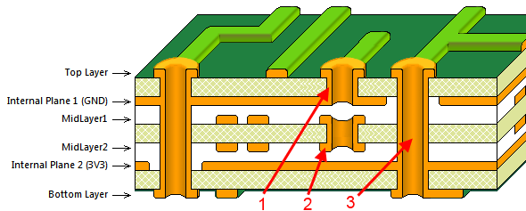
Vias are one of the important components of a multi-layer PCB, the cost of certain vias can be up to 30% to 40% of the total board cost. As we all know, printed circuit boards are superimposed by copper foil circuit layer upon layer, and the connection between the different circuit layers is provided by vias. An insulating layer is laid between each layer of copper foil, so that the copper foil layers are insulated from each other and signals are isolated to vias. The three most common vias are plated through-hole, blind hole and buried hole. Below are the details of these three kinds of PCB via hole.

In the figure above, 1 refers to Blind Via Hole(BVH), 2 refers to Buried Via Hole (BVH), and 3 refers to Plating Through Hole(PTH).
Plating Through Hole(PTH)
Plating through hole is the most common via, just take up PCB and face to the light, if you can see the light, then it is the “through hole”. PTH is also the simplest kind of hole because it just need to use drill or laser light to make a full borehole, and the cost is relatively cheap. But some circuit layer do not need plating through hole. Although PTH is much cheaper, sometimes, it may use some more PCB space.
Blind Via Hole(BVH)
Connect the outermost circuit of the PCB and the adjacent inner layer with plated through-hole, since we cannot see the opposite, so it is called “blind pass”. In order to increase the space utilization of PCB circuit layer, blind via hole came into being. Please note that this production method requires special attention to the depth of the hole (Z axis) should be appropriate. Almost no PCB manufacturer adopt this kind of method because the difficult of hole plating.
Buried Via Hole (BVH)
Buried via hole connects to any circuit layer of PCB but do not pass to the outer layer. This process cannot be done using the method of bonding after drilling, it must be in the individual circuit layer when the implementation of drilling, the first part of the internal bonding after the first plating treatment, and finally all the bonding. Buried via hold need more time than the original “through-hole” and “Blind hole”, so its’ price also the most expensive. This process is usually used in high-density (HDI) circuit boards to increase the other circuit layer can be used space.
The electroless copper deposition process is used for PCBs with two or more copper layers. However, designers have to be aware that not every hole and slot will be plated. Therefore, you must follow your manufacturer’s rules to know which will be plated and which will not.
